SENTECH and Mi-Net constantly collaborate with academic and industrial partners to research advanced processes and applications crucial for the semiconductor industry. This research aims to drive innovation, meet market demands, secure new revenue streams, and ensure long-term sustainability.
Dielectric layers such as silicon nitride (SiNₓ) and silicon dioxide (SiO₂) on silicon carbide (SiC) wafers are considered essential for next-generation technologies and have the potential for use in various industries including power electronics, telecommunications, and automotive electronics due to their superior electrical, thermal, and mechanical properties.
SiC possesses unique material properties such as high thermal conductivity, high breakdown voltage, and wide bandgap, making these substrates highly suitable for applications in harsh environments where traditional silicon devices may not perform reliably. However, the thickness of SiC wafers presents challenges in processes and applications. Meeting these challenges requires accurate characterisation, precise process quality control and optimisation of material defects, impurities, and interface properties crucial for assessing the reliability and yield of SiC-based semiconductor devices.
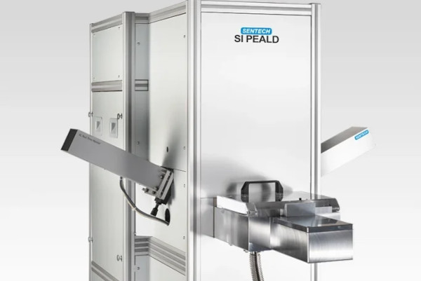
Ellipsometric characterisation serves as an efficient quality control and process optimisation measure during the fabrication of dielectric layers and stacks in SiC-based devices. This helps ensure that the required specifications and standards for a desired application are met efficiently. Ellipsometry is used as a non-destructive, highly accurate, and precise method for characterising dielectric layers such as SiO₂, SiNₓ, HfO₂, Al₂O₃, and photoresists on SiC substrates.
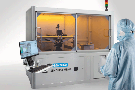
The SENTECH SENDURO®MEMS is a fully automated tool for measuring film thicknesses and optical constants to control etch and deposition processes. This versatile tool covers many applications on both patterned and non-patterned wafers. The system is equipped with a robot for automated wafer handling using wafer cassettes (100 mm, 150 mm, and 200 mm wafers) and a pre-aligner with a notch and flat finder for the pre-alignment of each wafer. Additionally, it can handle double-sided processed wafers using edge grip handling and includes an OCR reader for reading a wafer ID from top or bottom. Test patterns are identified by pattern recognition and adjusted precisely on the measurement point. Results and statistics can optionally be reported via SECS/GEM to an MES.
SENTECH has recently carried out successful process research demonstrating the measurement of dielectric layers on SiC wafers and has created a new application note. You can learn how non-invasive ellipsometry techniques accurately measured SiNₓ on a 100 mm SiC wafer with a 0.35 mm thickness.
You can request a pdf copy of this application note by clicking the Request Application Notes link below or you can email us at sales@mi-net.co.uk.