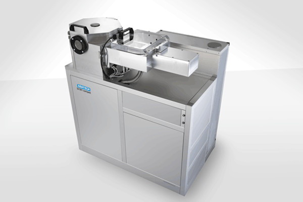
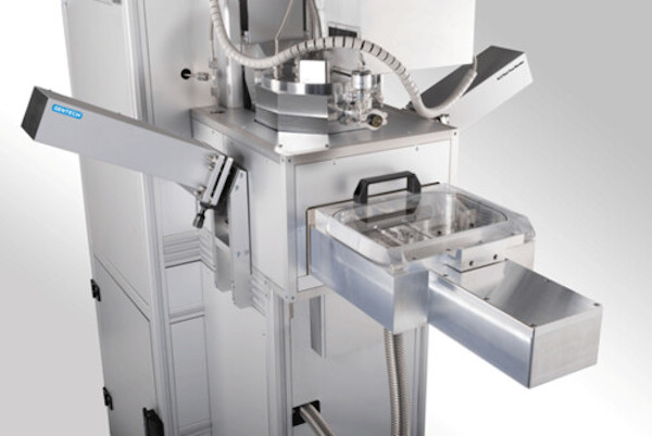
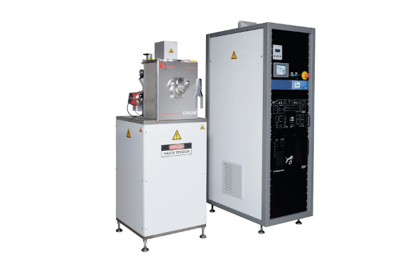
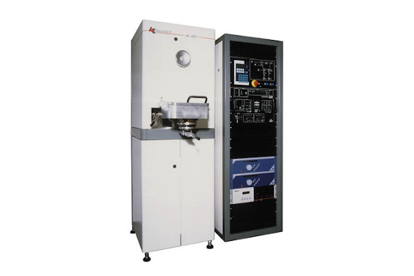
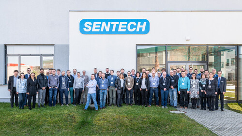
On April 25th 2024 SENTECH Instruments will host this years application oriented seminar on Plasma Process Technology. The seminar will take place at their Berlin HQ and will include a tour or the production and application labs at SENTECH. Speakers will present on topics relating to low damage etching and coating in the processing of compound semiconductor devices, for applications in the production of infra-red sensors, optics, power semiconductors and quantum technology.
On the evening before, April 24th at 7pm the participants are invited to a networking event at a restaurant in Berlin. The number of participants is limited so please contact us if you would like to reserve a space. The cost of the seminar is 300 euros per person.
Seminar Program
| 09:00 | Welcome and introduction of the program, organisation, and SENTECH employees Friedrich P. Witek, SENTECH GmbH, Krailling and SENTECH Instruments GmbH, Berlin |
| Etching: | |
| 09:10 | SENTECH Plasma Process Technology Latest developments in etching of LiNbO3, diamond structures, and stress-controlled ICPECVD Marcel Schulze, SENTECH Instruments GmbH, Berlin Friedrich P. Witek, SENTECH GmbH, Krailling and SENTECH Instruments GmbH, Berlin |
| 09:40 | Comparison of different PEALE modes on nitride semiconductors Christian Miersch, Fraunhofer-Institut für Integrierte Systeme und Bauelementetechnologie IISB, Außenstelle THM, Freiberg, Germany |
| 10:10 | Coffee break and time for discussions |
| 10:45 | Challenges in manufacturing of mid-infrared semiconductor devices Artur Trajnerowicz, Vigo System S.A., Ożarów Mazowiecki, Poland |
| 11:15 | In-situ depth control for plasma etching steps in optical III-V devices Ralph-Stephan Unger, Ferdinand-Braun-Institut gGmbH, Leibniz-Institut für Höchstfrequenztechnik, Berlin, Germany |
| 11:45 | Applications of DRIE using Bosch process and cryogenic etching for Silicon Seçkin Akıncı, Koç Üniversitesi, Istanbul, Türkiye |
| 12:15 | Lunch and time for discussions |
| Deposition: | |
| 13.45 | Multilayered optical coatings by PVD, ICPECVD, and PEALD combined in a single cluster Mario Ziegler, Leibniz-Institut für Photonische Technologien e.V. (IPHT), Jena, Germany |
| 14:15 | Advanced processing of large-area MoS2 layers in a five-chamber cluster tool for (flexible) 2D electronics Claudia Bock, Ruhr-Universität Bochum, Fak. für Elektrotechnik und Informationstechnik, LS f. Mikrosystemtechnik, Bochum, Germany |
| 14:45 | Coffee break and time for discussions |
| 15:20 | In-situ process development of HfO2, Al2O3, and AlN PEALD on SiC for power electronics Paul Plate, SENTECH Instruments GmbH, Berlin, Germany |
| 15:35 | PEALD for organic perovskites for solar applications Jakob Zessin, SENTECH Instruments GmbH, Berlin, Germany |
| 15:50 | The SENTECH PTSA ̶ a unique ICP plasma source Michael Höfner, SENTECH Instruments GmbH, Berlin, Germany |
| 16:30 | All participants of the seminar are invited to visit the application laboratories at SENTECH Instruments |
| 17:30 | End of the seminar |
