A comprehensive range of sputtering materials and sizes available
Micro machined components in strategic materials such as molybdenum, tantalum, titanium and niobium
Garnet crystals and substrates for epitaxy
We supply high purity evaporation materials for vacuum vaporation in a variety of shapes and sizes.
Indium and gallium antimonide. The InSb detectors are sensitive between 1 µm to 5µm wavelengths.
Czochralski (Cz) and float zone (Fz) for a large range of semiconductor applications
Scratch, indentation and wear testing all on one tool at nano and micro load ranges
3D non-contact profilometers for collecting and analysing sample height data
Robust, modular, and powerful pin on disc tribometers
Advanced 3D optical measurement solutions for quality assurance in production
Non-contact technology measuring real time strength and direction of electrical currents
Reproducing the wear interaction between a surface and the human finger
Measurement of surface tension between liquids and solids
Determining thin film properties by change in polarisation of light
Measuring thin film properties by reflection
Tribology testing in ambient or tailored environments
Real life testing of finished products in respect of resistance to hand abrasion
Scratch & indentation for hardness, elastic modulus, adhesion, cohesion plus more
Gain a deeper understanding of your materials
Measure surface roughness, form, profile, finish plus more
Low damage plasma enhanced chemical vapour deposition
Low damage etching and nano structuring
Deposition of layers in the nanometer scale
Deposition of coatings by the vacuum evaporation technique
Deposition of coatings by the sputtering technique
The dispersion, mixing, pulverization or emulsification of materials
Scintillator materials grown in crystal form
Scintillator material in organic form
Materials for the measurement of radiation dose
Sapphire in sheet, tube, rod and component form
LiF, Quartz or SiO2, InSb, Si, Ge, PET, ADP, Beryl, TlAP, RbAP, KAP and CsAP
Bespoke leak testing systems for small or large parts
High performance laser optics from Alpine Research Optics
Powerful, easy to use and cost effective AI based image recognition
A comprehensive solution for laboratories using several types of microscope and profilometer
Benchmark technology for 2D and 3D surface texture analysis and metrology, seamlessly integrates with profilometers and other surface measuring equipment
Conductive coating on one side to prevent EMI/RFI
Plastic optical filter with broadband AR coating on both sides
Privacy Glass & Light Control Film
J-GRAPHENE is a graphene dispersion developed by Jokoh of Japan using their high pressure NAGS homogeniser. It is a high quality, low defect graphene dispersion with high heat and electrical conductivity that provides a level of performance comparable to carbon nanotubes.
J-GRAPHENE was designed to be high quality whilst being easy to use and affordable.
Full production is due to start in 2026, but you can contact us now for samples.
Jokoh of Japan have been part of healthcare research and development for over 70 years. They opened their first branch in Tokyo and now market their products to approximately 40 countries worldwide. In recent years they have expanded their portfolio with the introduction of the NAGS homogeniser and more recently the exciting J-GRAPHENE liquid dispersion material.
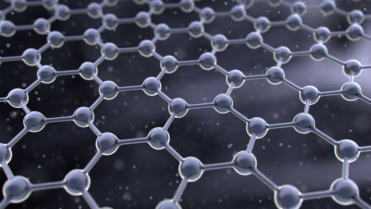
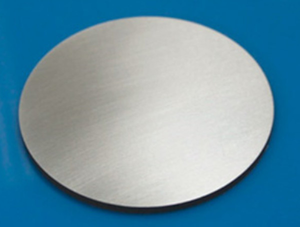
Graphene is called the ultimate carbon nano-material, but there were two challenges in developing it compared to others.
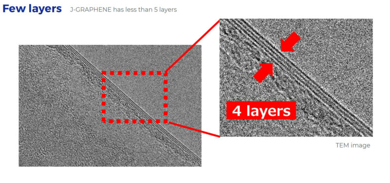
The first was the problem of quality. Since graphene requires complex and intricate structuring, achieving a low level of defects is difficult.
The second was the problem of cost. Due to the processing required to manufacture graphene, cost was also a challenge.
This is probably a reason some companies are forced to give up on using graphene and find a substitute even though they understand its utility. Since it’s difficult for companies to use graphene at present, this is inhibiting business and technology innovation.
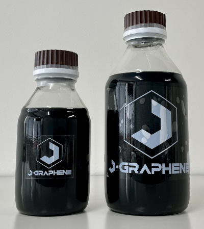
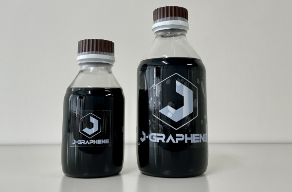
To solve this problem, Jokoh have made this dream material more approachable with J-GRAPHENE. While maintaining low defects and high quality, J-GRAPHENE was developed with a commitment to low cost and high usability.
J-GRAPHENE is sure to be useful to both startups proposing new value and improved functionality or cost reduction for existing products.
Graphene type | Few layer graphene (FLG) |
Form | Dispersion (NMP) |
Manufacturing method | Liquid phase exfoliation |
Raw material | Natural graphite |
Graphene concentration (wt%) | 1.0 |
Solvent content (wt%) | 99.0 |
Product | JKG04 |
Structural defects (ID/IG) (Raman) | <0.20 |
Number of layers (Raman) | <5 |
Lateral dimensions (μm) | <3.0 |
J-GRAPHENE has less then 5 layers with drastically lower defect rates compared to other materials.
The applications for J-GRAPHENE are wide ranging and include:
Other products within the Semiconductor Materials part of our range
We’re here and ready to provide information and answers to your questions
©Mi-Net 2023. All Rights Reserved.
Website by Fifteen.co.uk