A comprehensive range of sputtering materials and sizes available
Micro machined components in strategic materials such as molybdenum, tantalum, titanium and niobium
Garnet crystals and substrates for epitaxy
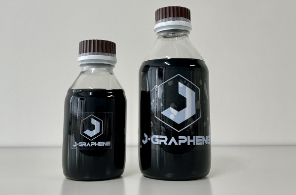
J-GRAPHENE is ahigh quality, low defect graphene dispersion
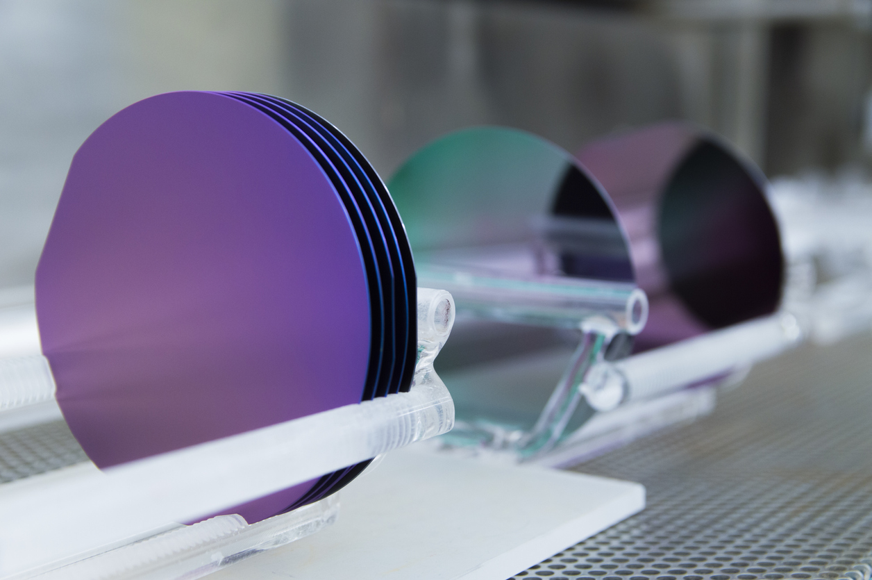
Czochralski (Cz) and float zone (Fz) for a large range of semiconductor applications
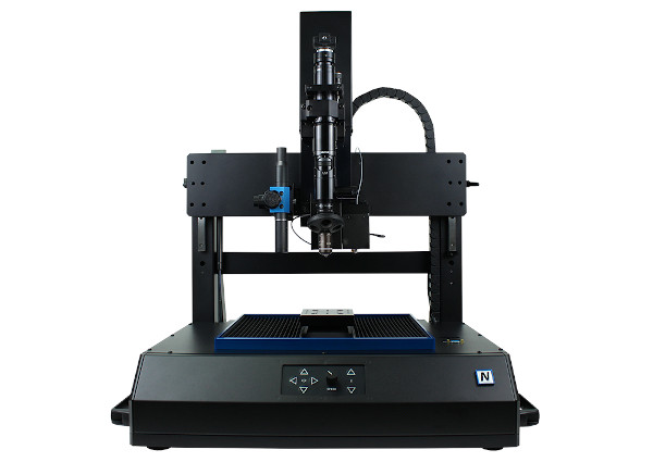
Scratch, indentation and wear testing all on one tool at nano and micro load ranges
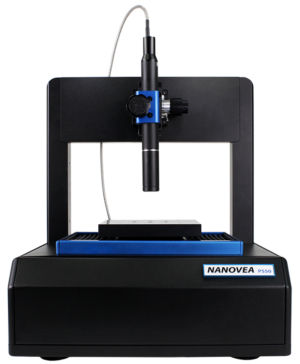
3D non-contact profilometers for collecting and analysing sample height data
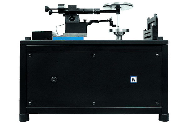
Robust, modular, and powerful pin on disc tribometers
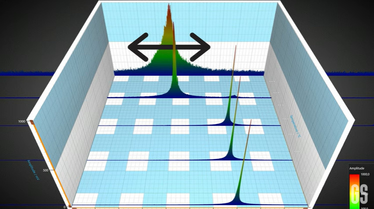
Non-destructive measurement of internal material properties
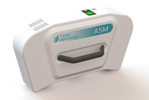
Advanced 3D optical measurement solutions for quality assurance in production

Non-contact technology measuring real time strength and direction of electrical currents
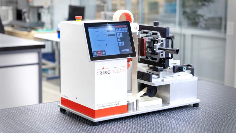
Reproducing the wear interaction between a surface and the human finger
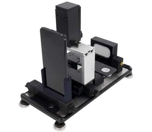
Measurement of surface tension between liquids and solids
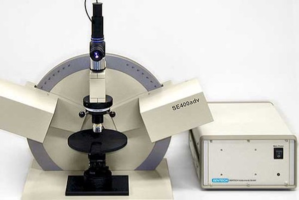
Determining thin film properties by change in polarisation of light
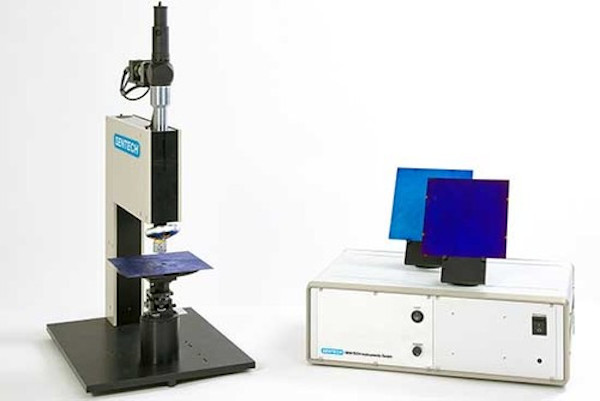
Measuring thin film properties by reflection
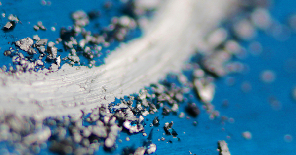
Tribology testing in ambient or tailored environments

Real life testing of finished products in respect of resistance to hand abrasion
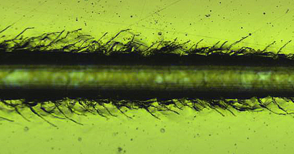
Scratch & indentation for hardness, elastic modulus, adhesion, cohesion plus more
Gain a deeper understanding of your materials
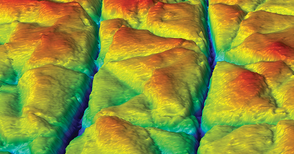
Measure surface roughness, form, profile, finish plus more
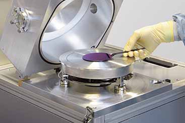
Low damage plasma enhanced chemical vapour deposition
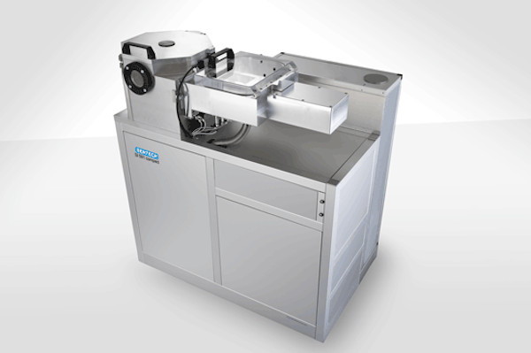
Low damage etching and nano structuring
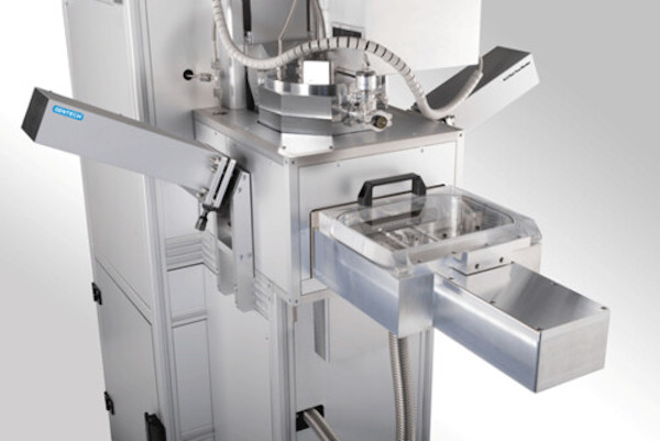
Deposition of layers in the nanometer scale
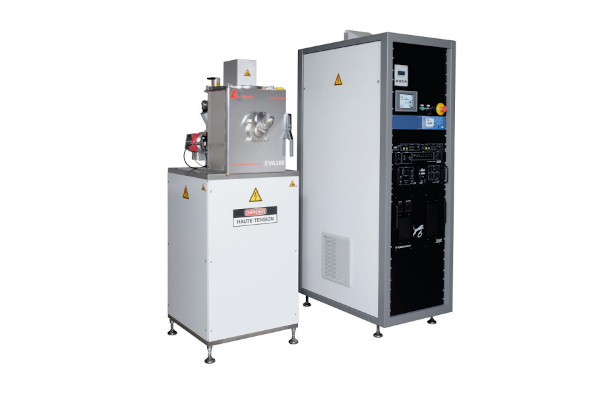
Deposition of coatings by the vacuum evaporation technique
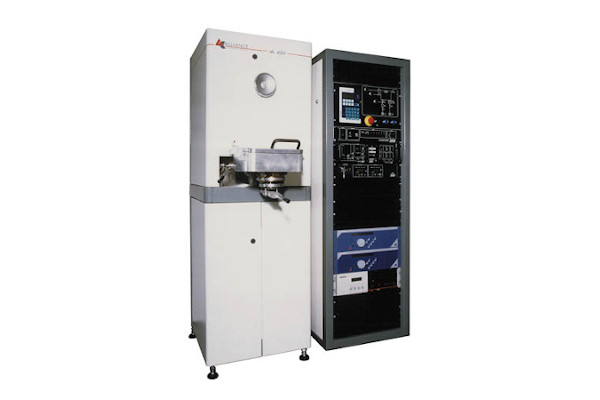
Deposition of coatings by the sputtering technique
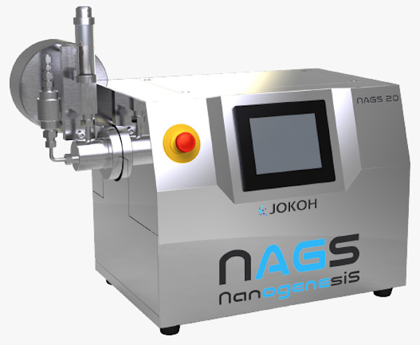
The dispersion, mixing, pulverization or emulsification of materials
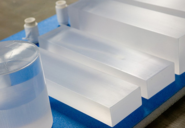
Scintillator materials grown in crystal form
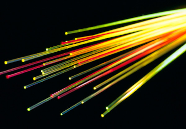
Scintillator material in organic form
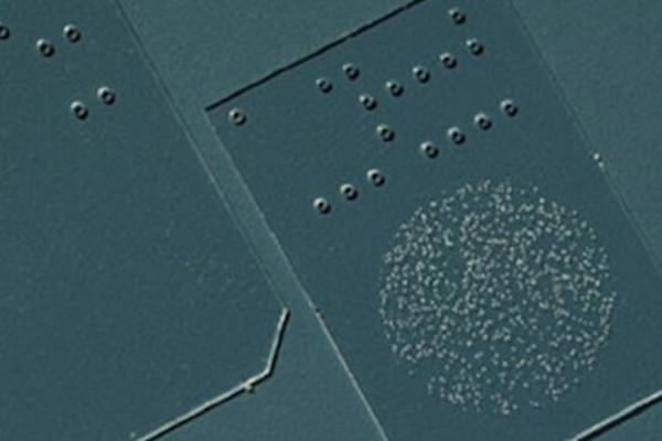
Materials for the measurement of radiation dose
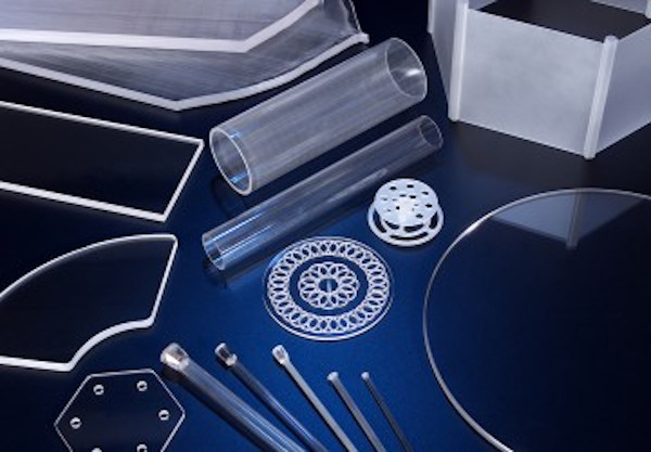
Sapphire in sheet, tube, rod and component form
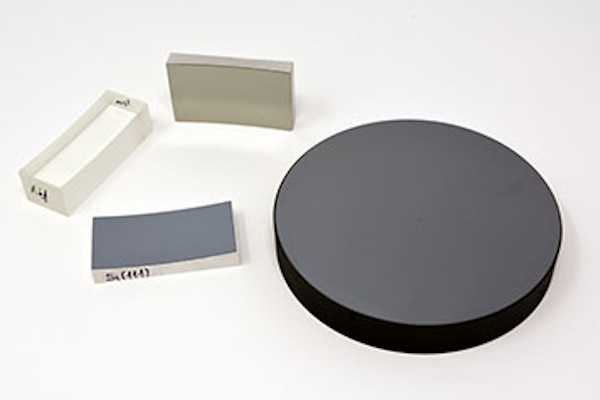
LiF, Quartz or SiO2, InSb, Si, Ge, PET, ADP, Beryl, TlAP, RbAP, KAP and CsAP
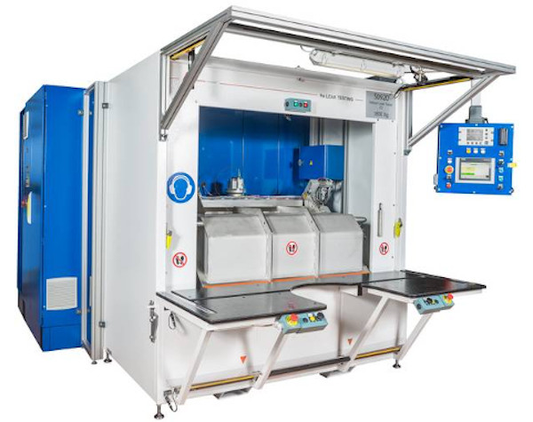
Bespoke leak testing systems for small or large parts
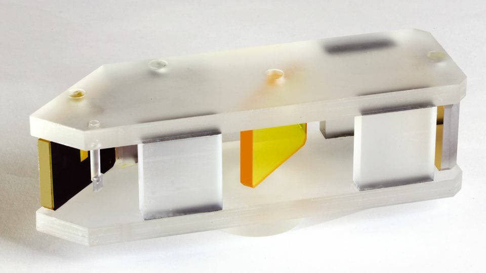
Superb optical stability and unsurpassed shock and vibration resistance
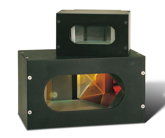
The performance of a penta prism with more control and wavelength transmission
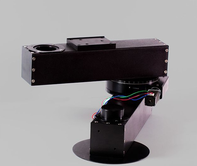
Beam alignment where three or more optical axes are required
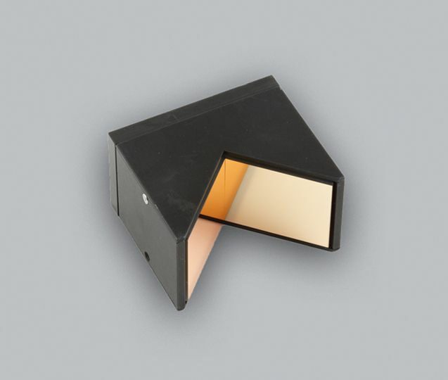
Two-mirror optical assembly arranged at a 90-degree angle
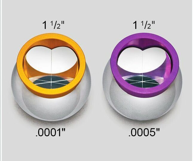
Ball mounted hollow retroreflectors
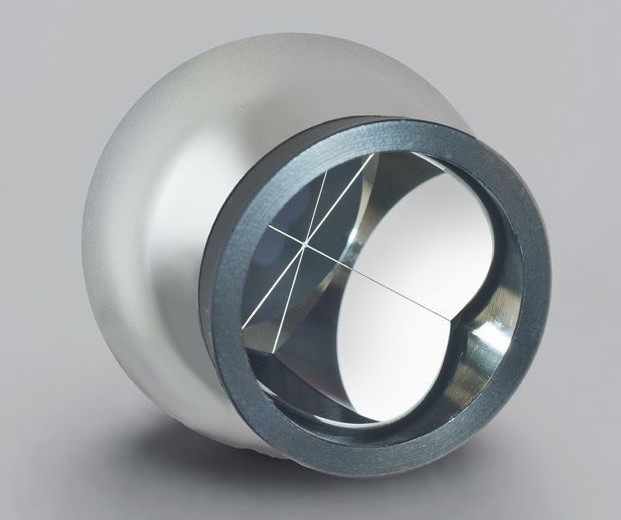
Reflects light back towards it’s source with minimal scattering

A comprehensive solution for laboratories using several types of microscope and profilometer

Benchmark technology for 2D and 3D surface texture analysis and metrology, seamlessly integrates with profilometers and other surface measuring equipment
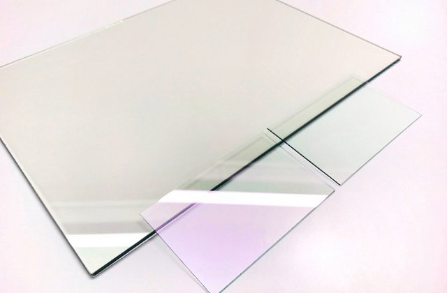
Conductive coating on one side to prevent EMI/RFI
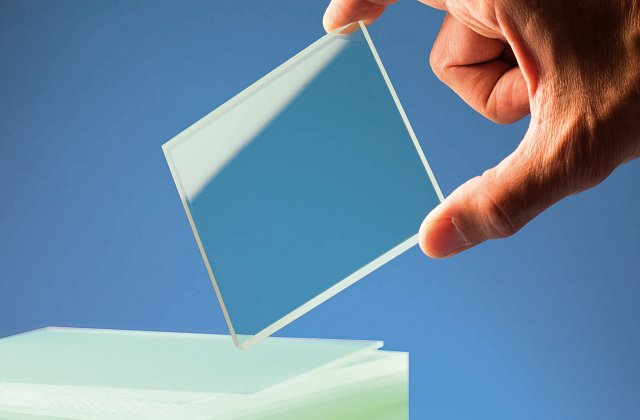
Plastic optical filter with broadband AR coating on both sides
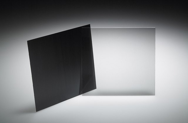
Privacy Glass & Light Control Film
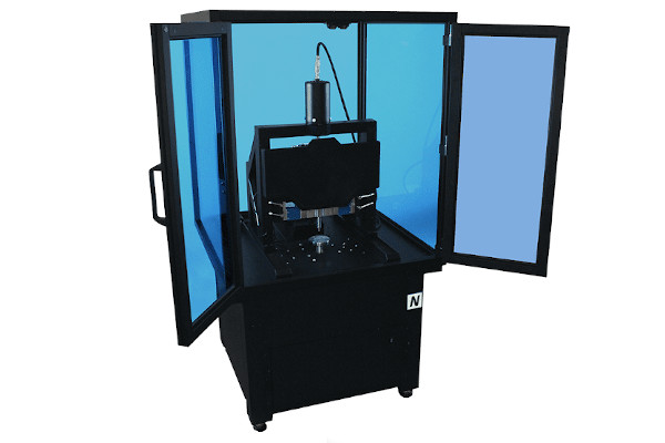
The T2000 pneumatic tribometer from Nanovea is designed to deliver cutting edge pin on disc tribology with a range of extra capabilities.
With a variety of test and environmental configurations available up to loads of 2000N the T2000 has been designed with flexibility and advanced requirements in mind.
High end options include innovative dual controlled loading, in-situ microscopes and a high speed profilometer.
Nanovea Inc are based in Irvine, a tech hub of Southern California. They have been redefining standards in quality control and materials development internationally for over a decade. Nanovea’s instruments can be found in renowned education and industrial organisations around the world.

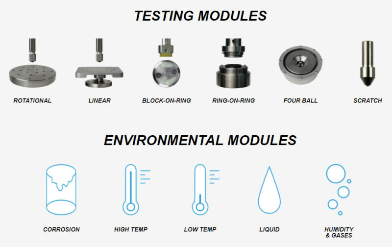
The T2000 is truly modular meaning you can start with test and environmental modules or easily add them later. There is no need to buy more than one tribometer for different tests and conditions because all can be completed on one T2000. In addition there are advanced optical options such as an in-situ microscope or high speed 3D profilometer available.
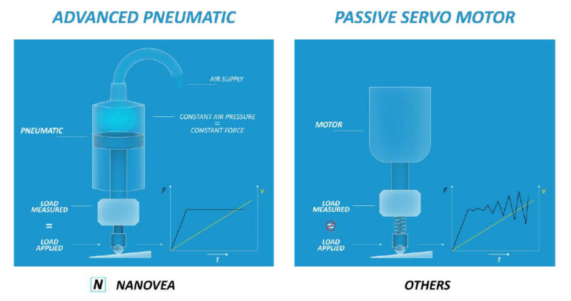
New Nanovea tribometers utilise advanced pneumatic loading technology to apply the vertical load onto a sample. This technology allows the tribometer to apply a constant force that is not badly influenced by changes in the sample topography. Pneumatic technology has an inherent natural dampening effect which further contributes to this constant force.
Pneumatic loading is computer controlled contributing to ease of use, allowing a greater deal of automation and allowing the addition of modes requiring load ramping such as scratch testing.
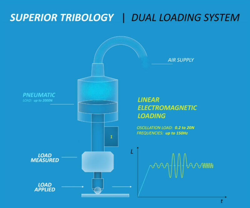
In addition a second linear stage can be used to apply a second oscillating load to simulate fluctuation of the overall load at frequencies up to 150Hz. This allows users to recreate real life applications where loads are not necessarily constant.
| Min/Max Testing Loads | 0.5N-2000N |
| Load Resolution | 0.12mN |
| Loading Type | Advanced Pneumatic |
| Frictional Force Maximum | Resolution | (+/-)1000N | 6µN |
| Fatigue Loading | 0.2 to 20N |
| Frequency of Oscillation | up to 150Hz |
| X Motorized Travel | 250mm |
| Max Rotational Speed | 5000rpm (optionally 15,000rpm) |
| Min Rotational Speed | 0.01rpm (0.05rpm with 15,000rpm motor) |
| Rotational Speed Acceleration (0 to 1000rpm) | 0.45 seconds (0.15 seconds with 15,000rpm motor) |
| Disc Size / Sample Mounting Area | 100mm diameter |
| Linear Stroke Range | 25mm |
| Maximum Linear Frequency (up to 5mm stroke) | 60Hz |
| Linear Mounting Area | 62 x 76mm |
| Max Scratch Length | 50mm |
| Scratch Speed | 0.002-10mm/s |
| Scratch Loading Rate | 1-200N/min |
| In-Situ 3D Profilometer | Standard or High Speed |
Nanovea regularly document and publish work using their tribometers. We keep many of these resources on our website in the form of application notes or publications. These are a great way to learn more about what can be achieved with a Nanovea tribometer.


Products related to the Nanovea T2000 tribometer.
We’re here and ready to provide information and answers to your questions
©Mi-Net 2023. All Rights Reserved.
Website by Fifteen.co.uk