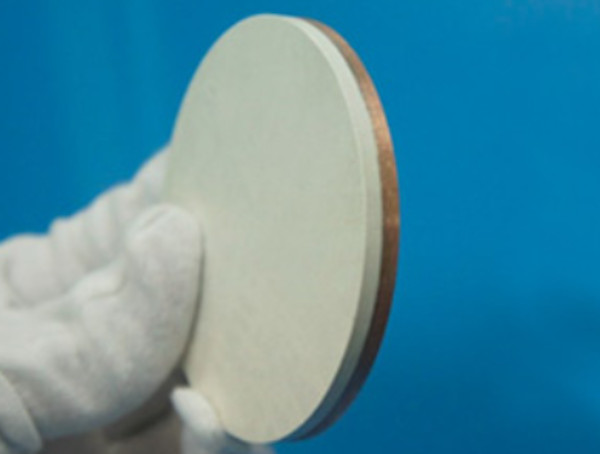
A comprehensive range of sputtering materials and sizes available
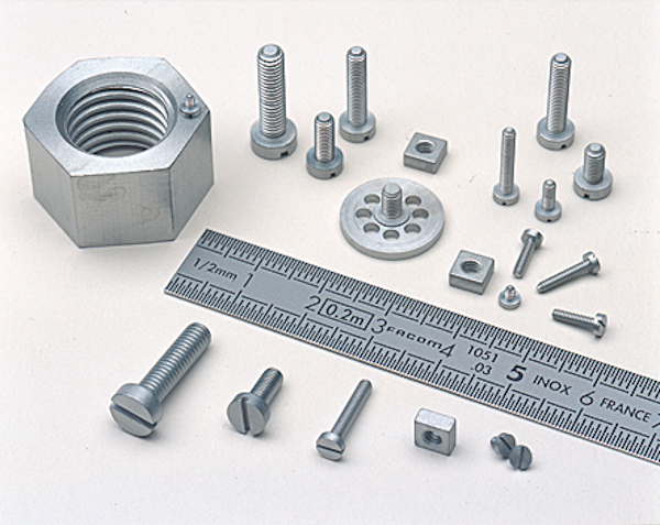
Micro machined components in strategic materials such as molybdenum, tantalum, titanium and niobium
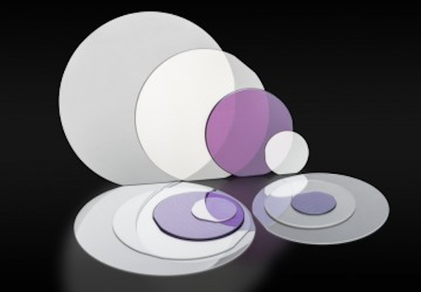
Garnet crystals and substrates for epitaxy
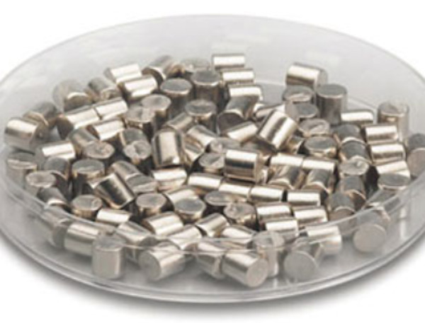
We supply high purity evaporation materials for vacuum vaporation in a variety of shapes and sizes.
Indium and gallium antimonide. The InSb detectors are sensitive between 1 µm to 5µm wavelengths.
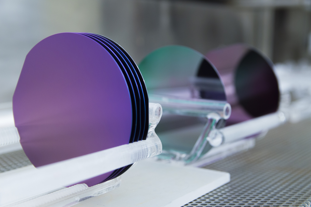
Czochralski (Cz) and float zone (Fz) for a large range of semiconductor applications
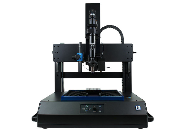
Scratch, indentation and wear testing all on one tool at nano and micro load ranges
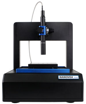
3D non-contact profilometers for collecting and analysing sample height data
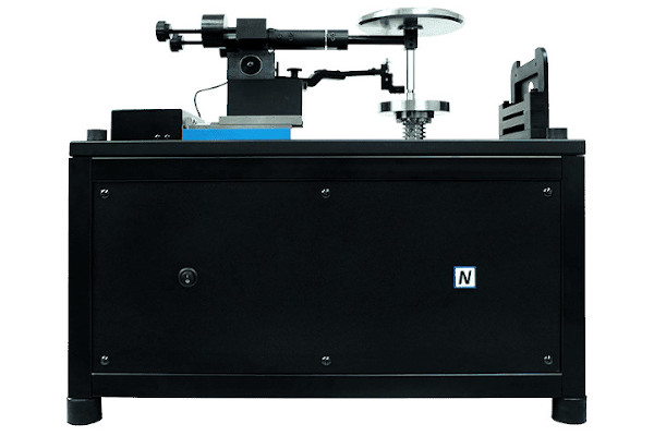
Robust, modular, and powerful pin on disc tribometers
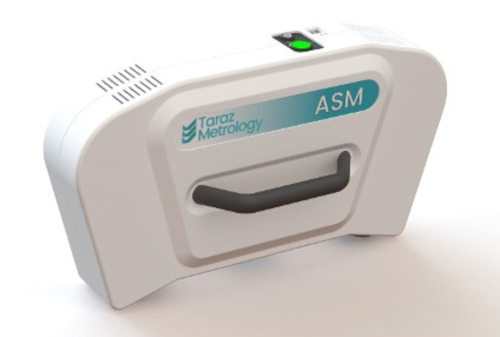
Advanced 3D optical measurement solutions for quality assurance in production

Non-contact technology measuring real time strength and direction of electrical currents
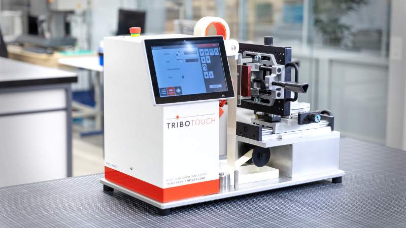
Reproducing the wear interaction between a surface and the human finger
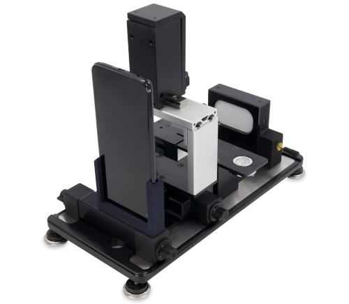
Measurement of surface tension between liquids and solids
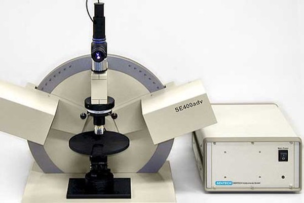
Determining thin film properties by change in polarisation of light
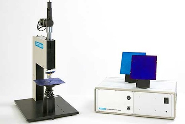
Measuring thin film properties by reflection
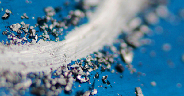
Tribology testing in ambient or tailored environments

Real life testing of finished products in respect of resistance to hand abrasion
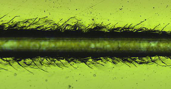
Scratch & indentation for hardness, elastic modulus, adhesion, cohesion plus more
Gain a deeper understanding of your materials
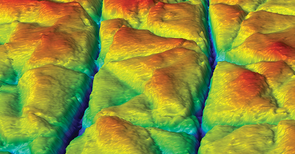
Measure surface roughness, form, profile, finish plus more
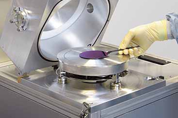
Low damage plasma enhanced chemical vapour deposition
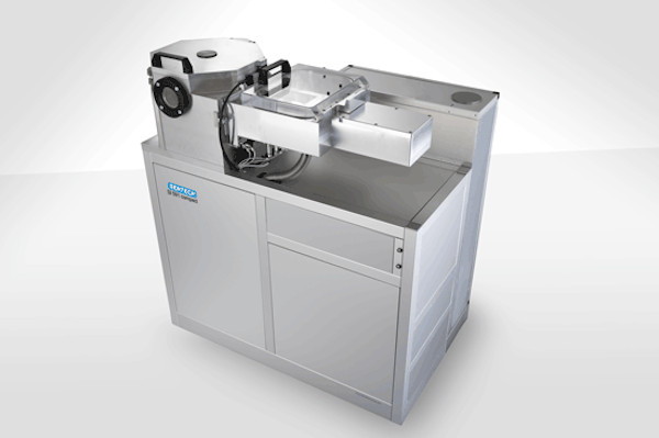
Low damage etching and nano structuring
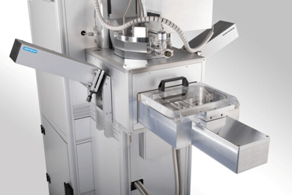
Deposition of layers in the nanometer scale
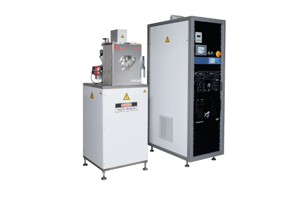
Deposition of coatings by the vacuum evaporation technique
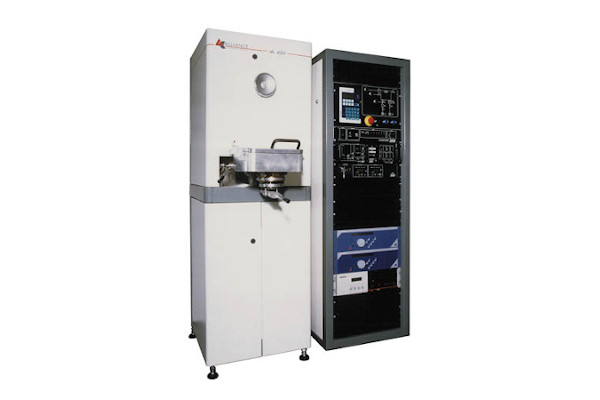
Deposition of coatings by the sputtering technique
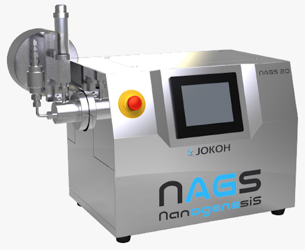
The dispersion, mixing, pulverization or emulsification of materials
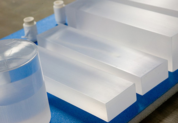
Scintillator materials grown in crystal form
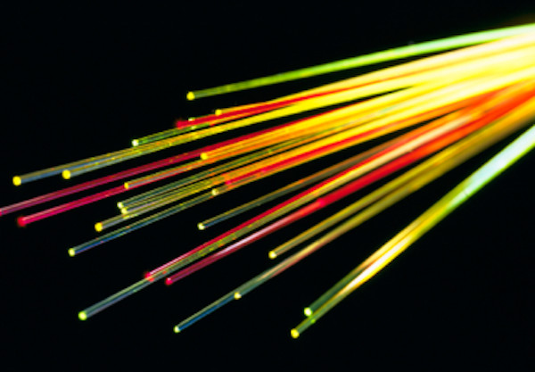
Scintillator material in organic form
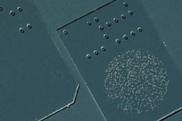
Materials for the measurement of radiation dose
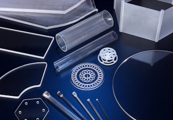
Sapphire in sheet, tube, rod and component form
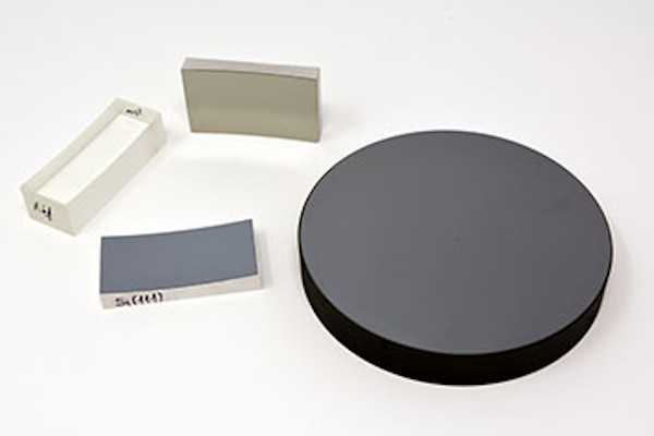
LiF, Quartz or SiO2, InSb, Si, Ge, PET, ADP, Beryl, TlAP, RbAP, KAP and CsAP
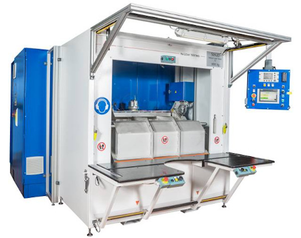
Bespoke leak testing systems for small or large parts

High performance laser optics from Alpine Research Optics

Powerful, easy to use and cost effective AI based image recognition

A comprehensive solution for laboratories using several types of microscope and profilometer

Benchmark technology for 2D and 3D surface texture analysis and metrology, seamlessly integrates with profilometers and other surface measuring equipment
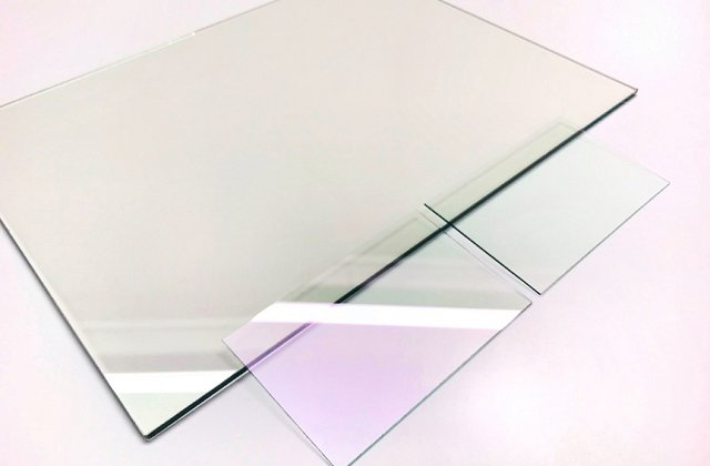
Conductive coating on one side to prevent EMI/RFI
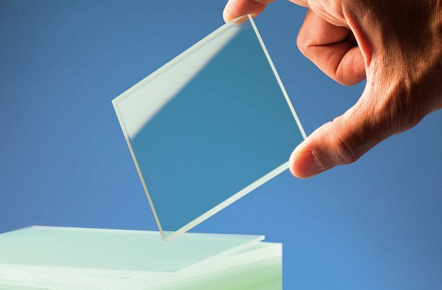
Plastic optical filter with broadband AR coating on both sides
Privacy Glass & Light Control Film

We supply X-ray monochromator crystals from Luxium Solutions (previously Saint Gobain Crystals). A monochromating crystal behaves in X-ray spectrometry as does a diffraction grating in optics therefore when rotated with respect to the incident beam it will diffract the spectral component in accordance with Bragg’s Law. The most important characteristic of a monochromating crystal is the double atomic spacing 2d, which defines the largest wavelength which can be diffracted. The St Gobain Crystals & Detector’s range of synthetic & naturally occurring monochromating crystals offers the widest possible variety of 2d spacing.
Our monochromating crystals are supplied as flat (unmounted or mounted on holders) for XRF spectrometers, or curved onto a holder to allow focusing for instruments such as microprobes, scanning electron microscopes, syncrotrons, XFEL, plasma physics.
Luxium Solutions (previously Saint Gobain Crystals) are the premier scintillation detection manufacture for ionizing radiation detection and provide high quality scintillation materials with superior resolution and advanced photo-sensor integration. Their core technology is the manufacturer of high performance engineering materials to solve their customers’ unique challenges. Luxium Solutions and Mi-Net have been working together in the UK and Ireland for over 30 years.

There are two main types of focusing configurations available:
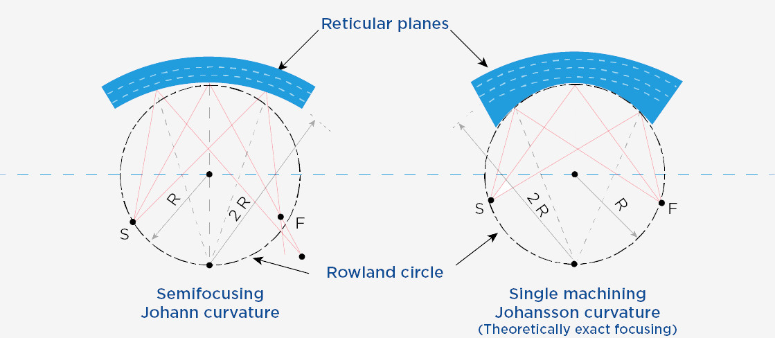
The Johann Geometry (semi-focusing)
A thin plate is produced by one of the two following methods:
The thin plate is then curved cylindrically and glued to a curved holder with approximate focusing.
The Johansson Geometry (exact focusing geometry)
Two different types of Johansson configurations, theoretically leading to perfect focusing, are considered:
The thin plate is either curved cylindrically, glued to a curved holder and one face is machined (single machining Johansson) or both faces are machined and then glued to a curved holder (double machining Johansson).
We will offer the best technique according to the type of crystal, its dimensions and the radius of Rowland circle to be achieved.
Other types of curvature may be investigated on request. Following designs can be made: Logarithmic spiral, Elliptical, Conical, Parabolic, Sphere, Toroidal
Manufacturing capabilities strongly depend upon the crystal nature, dimensions as well as the curvature radii.
| Crystal | Lithium fluoride | Quartz | Indium Antimonide | Silicon | Germanium | Pentaerythritol PET | Ammonium Dihydrogen Phosphate ADP | Beryl | Acid Phthalates | Crystal | ||||||||
|---|---|---|---|---|---|---|---|---|---|---|---|---|---|---|---|---|---|---|
| Thallium TIAP | Rubidium RbAP | Potassium KAP | Cesium CsAP | |||||||||||||||
| Chemical Formula | LiF | SiO2 | InSb | Si | Ge | C(CH2OH2) | NH4H2PO4 | 3BeO,Al2O36SiO2 | CO2HC6H4CO2TI | CO2HC6H4CO2Rb | CO2HC6H4CO2K | CO2HC6H4CO2Cs | Chemical formula | |||||
| Crystal system | Cubic | Hexagonal | Cubic | Cubic | Cubic | Quadratic | Quadratic | Hexagonal | Orthorhombic | Orthorhombic | Orthorhombic | Orthorhombic | Crystal System | |||||
| Parameters | Parameters | |||||||||||||||||
| a………………Å…. | 4.027 | 4.913 | 6.48 | 5.431 | 5.658 | 6.16 | 7.530 | 9.21 | 6.63 | 6.55 | 6.46 | 6.580 | a………………Å…. | |||||
| b………………Å…. | 4.913 | 6.16 | 7.530 | 9.21 | 10.54 | 10.02 | 9.61 | 10.752 | b………………Å…. | |||||||||
| c………………Å…. | 5.405 | 8.74 | 7.542 | 9.17 | 12.95 | 13.06 | 13.33 | 12.825 | c………………Å…. | |||||||||
| ß…………………… | ß…………………… | |||||||||||||||||
| Reflecting planes orientations | (200) | (220) | (420) | (1011) | (1010) | (111) | (111) | (220) | (111) | (220) | (002) | (101) | (1010) | (001) | (001) | (001) | (001) | Reflecting planes orientations |
| 2d in Å | 4.027 | 2.848 | 1.801 | 6.684 | 8.514 | 7.480 | 6.271 | 3.840 | 6.532 | 4.000 | 8.740 | 10.648 | 15.950 | 25.900 | 26.120 | 26.640 | 26.650 | 2d in Å |
| Usual surface finish | Cleaved or Treated | Treated | Treated | Polished | Polished | Polished | Polished | Polished | Polished | Polished | Cleaved or Treated | Polished or Treated | Polished | Cleaved | Cleaved | Cleaved | Cleaved | Usual surface finish |
| Reflectivity | Intense | Intense | Average | Good | Good | Intense | Intense | Average | Intense | Intense | Intense | Average | Average | Intense | Intense | Good | Good | Reflectivity |
| Calibration elements | Mo, Fe, Ti | Mo, Fe | Mo | Cu | Cu | Si | Cu | Cu | Cu | Cu | Al, Si | Mg | Mg | Na, Mg | Na | Na | Na | Calibration elements |
| Common Applications | From K to heavy elements | Heavy elements Lines splitting |
Heavy elements Lines splitting |
As Ge (111) |
As PET | Quantitative analysis of silicon | Extinction of even order spectral lines | Mg | Na and following elements | F to Al | Na to Al, up to F in emission probes | Na to Al, up to F in emission probes | Na to Al, up to F in emission probes | Common applications | ||||
We’re here and ready to provide information and answers to your questions
©Mi-Net 2023. All Rights Reserved.
Website by Fifteen.co.uk